CVB3 Calculator
-
The goals for this project were the following:
Create a device capable of running on dual CR2032 batteries for over a year.
Create a reverse polish notation (RPN) calculator containing a standard set of features (listed below).
Create a menu based UI with a 400×240 pixel display.
Create a programming interface contained entirely on the device.
Keep the cost-per-unit under $100 for a small batch of 100 calculators.
-
The primary purpose of this project was to focus on low power design. This would be achieved by selecting low power components and making use of stop modes on the MCU. The largest saving came from the display, a 400×250 pixel SHARP Memory LCD (LS027B7DH01A), and the primary computation unit: the STM32L452RCT6.
The LS027B7DH01A display is theoretically capable of displaying and updating information while drawing consistently under ~50uA at 5V.
The STM32 MCU draws ~1.5uA in stop 2 mode, which retains RAM and is the mode that the calculator will be in while waiting for input, or while ‘off’. During periods of computation, the STM32 is clocked at 4MHz and draws under 1mA.
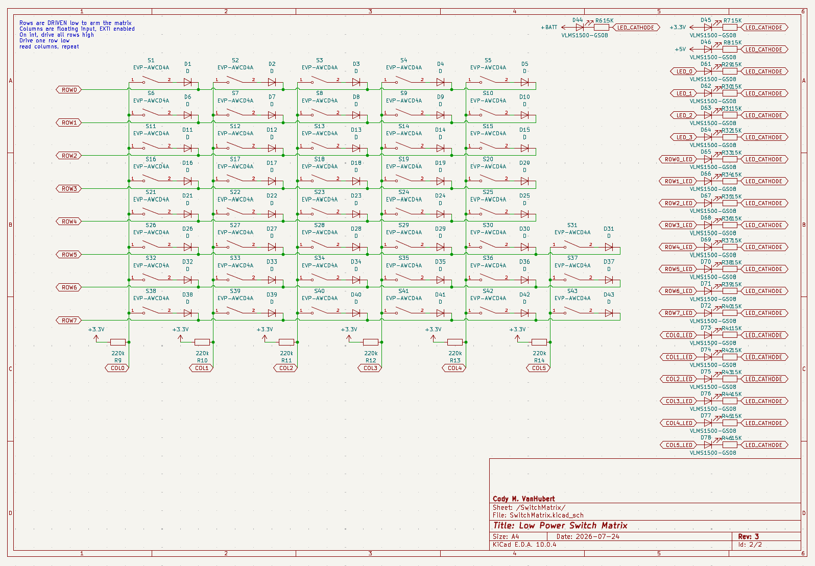
The highest current draw within the device is the wettng current for the front facing switches. This current is 3.3mA and only happens momentarily due to the scanning logic I have implemented.
-
In order to properly test the low power operation of the device, I wanted to create a fully featured RPN calculator. Simple addition, subtraction, multiplication, and division would be trivial to do without consuming much energy, so the following set served as the absolute minimum capability goal for this project:
Decimal math computation. On board FPU will not be utilized for most math operations.
Dedicated exponent, reciprocal, root, log, and natural log keys.
Trigonometric operations, as well as inverse functions, with dedicated keys.
Summation, integration, and linear regression functionality.
Scientific and engineering notations.
Uncertainty propagation for repeated calculations.
Simple complex number entry.
On-board programming interface similar to the HP35S.
PCB Design
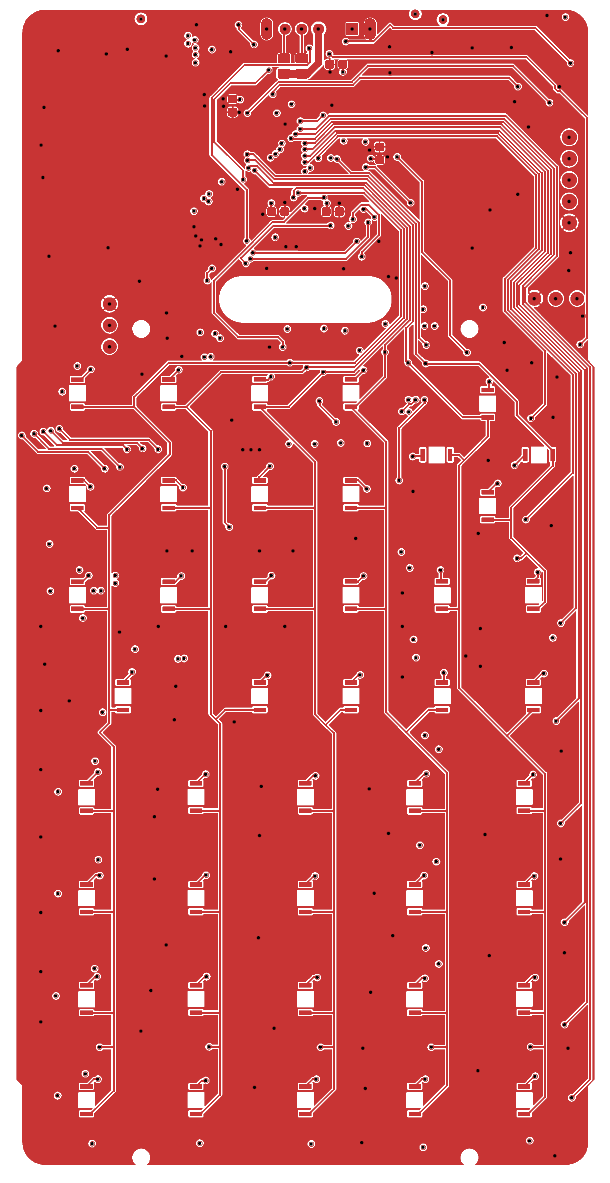
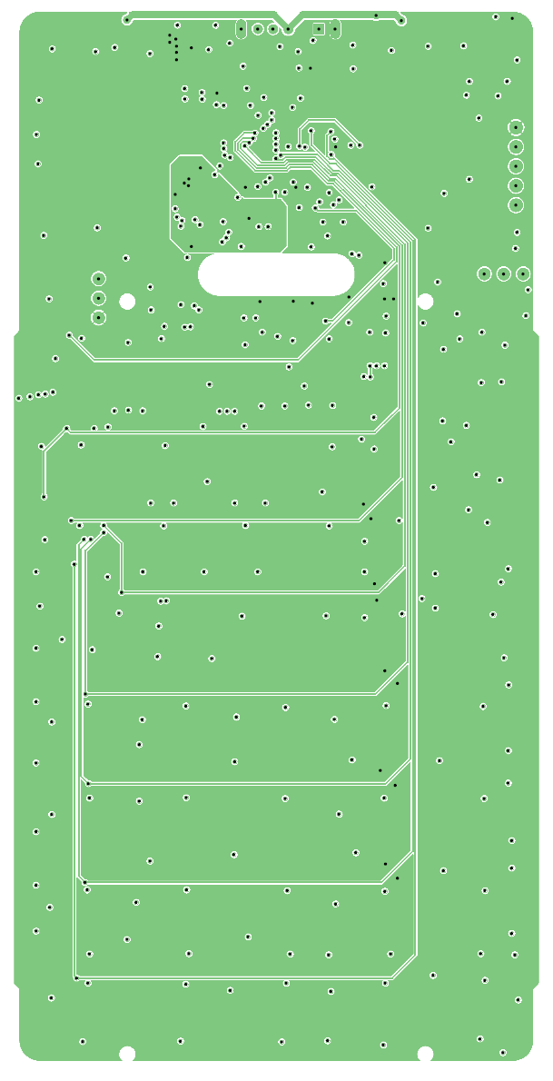
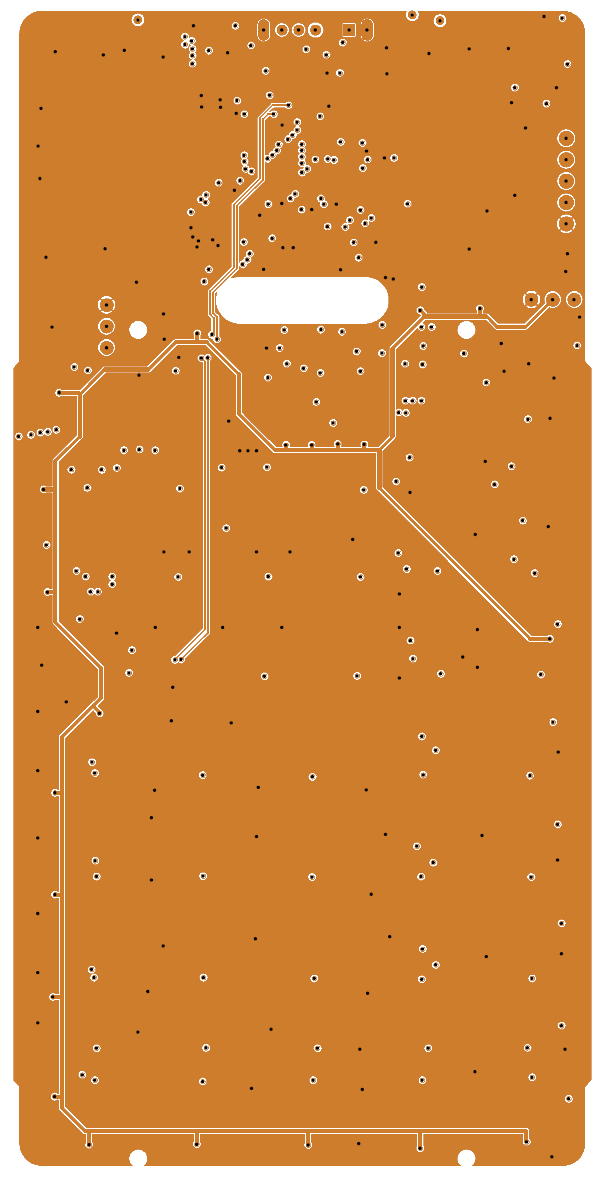
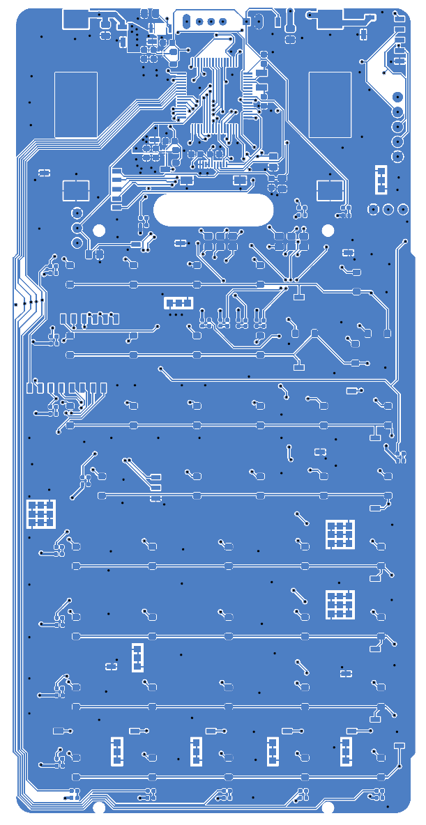
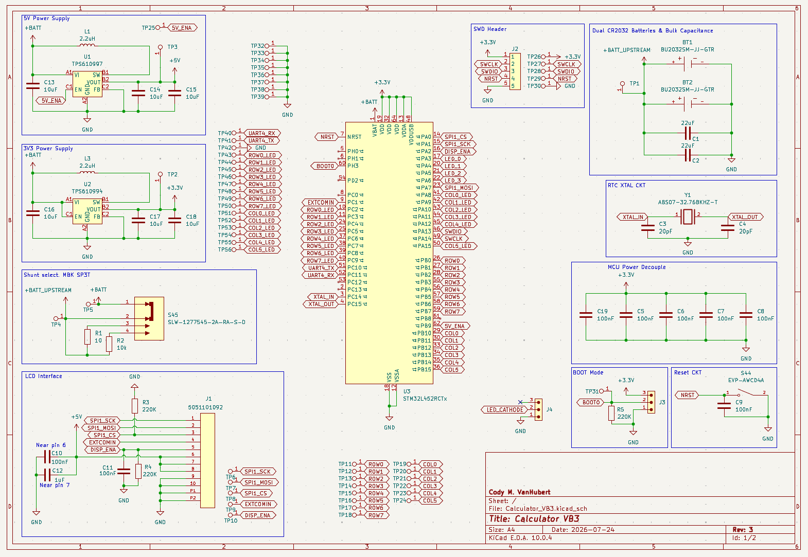
The PCB is a four layer PCB designed in KiCAD. The stackup is the standard “no requirements”, 1.6mm four layer option offered by JLCPCB. There are no differential pairs or impedance matched signals on the PCB, and there are no signals exceeding 2MHz.
This is a prototype PCB, so many of the components are populated for testing. All LEDs, test points, SWD programming header, LED and BOOTMODE headers, and the shunt resistors/selector switch can be omitted in a production version of the board.
The board also includes fiducial markers, three on the bottom and four on the top, for a future pick-and-place machine of mine.
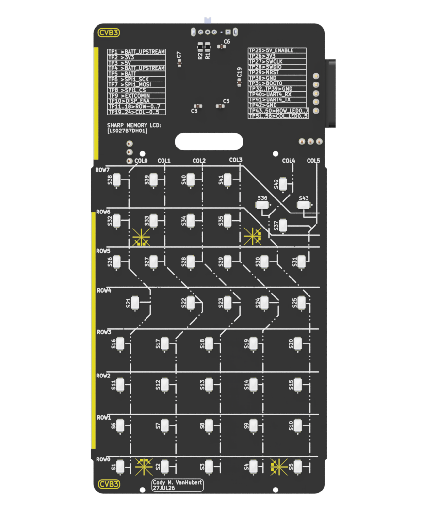
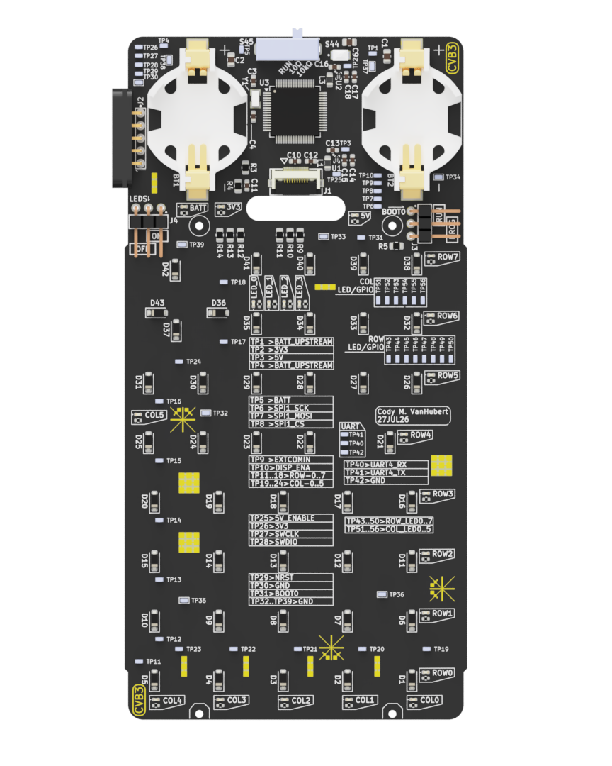
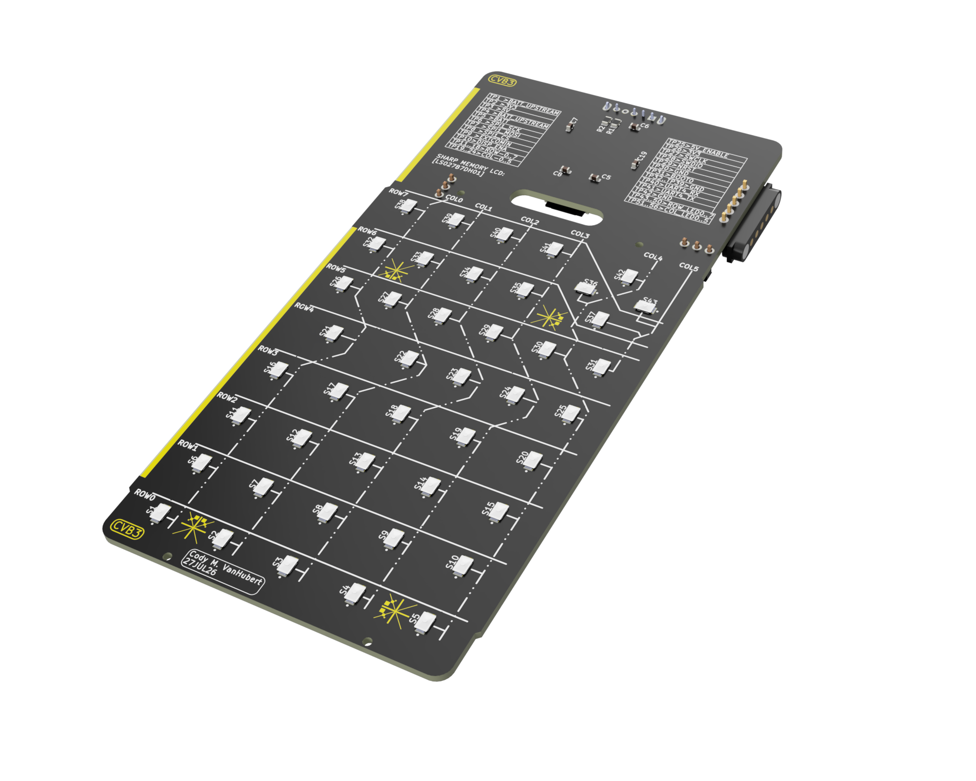
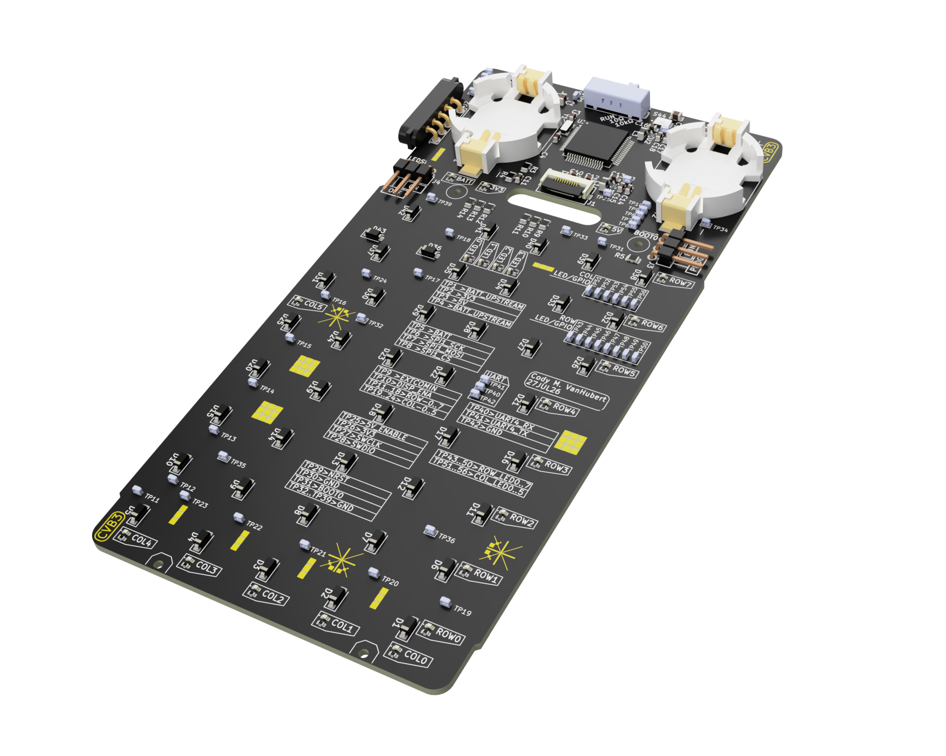
Layers: Top, Power, Ground, Bottom
Schematic Pages
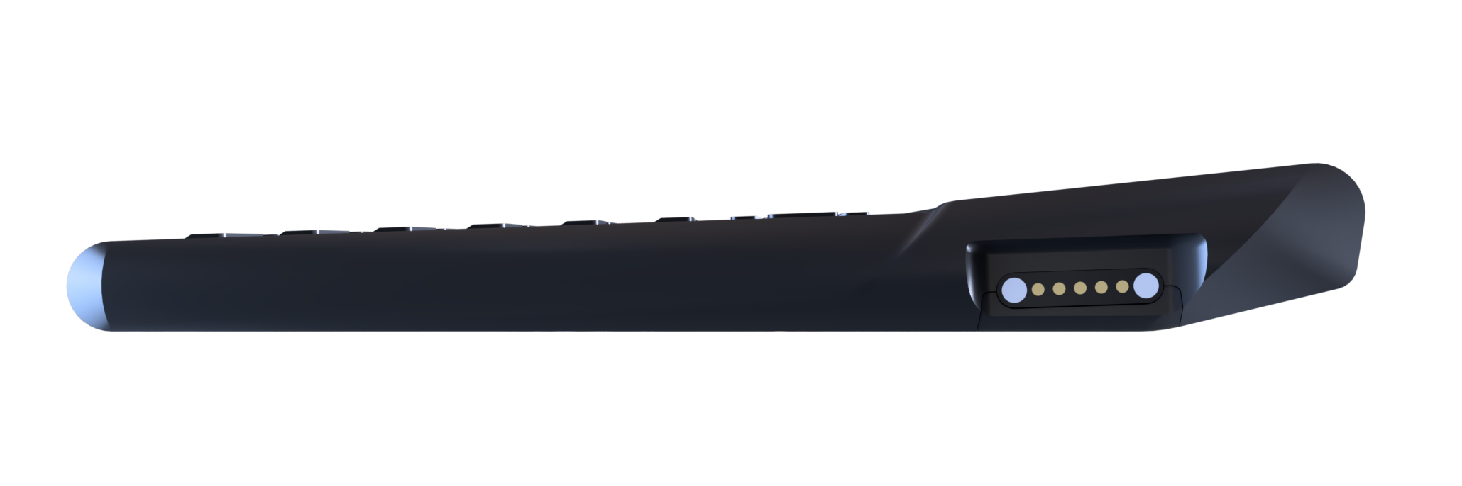
The enclosure for the board was designed in Fuson360. The enclosure was designed to be fabricated using an SLA process through JLC3DP. All parts were designed to make use of 3D printing such that they can be used to create silicone molds to cast future enclosures from semi-rigid polyurethane. As designed, the tolerance is slightly loose (~0.3mm between parts) to allow for a passive coating to keep the resin from inhibiting the silicone cure.
Designing this way allows me to make medium batches of cost-effective parts without needed to invest in an injection mold or hand finish a medium to high volume of 3D printed parts.
Fabrication and Cost
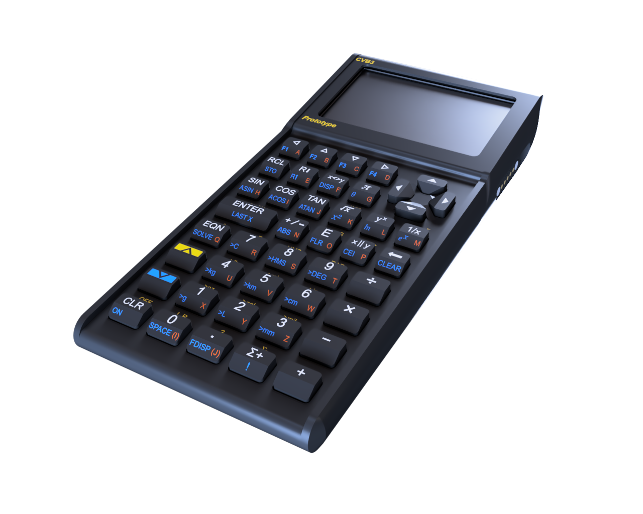
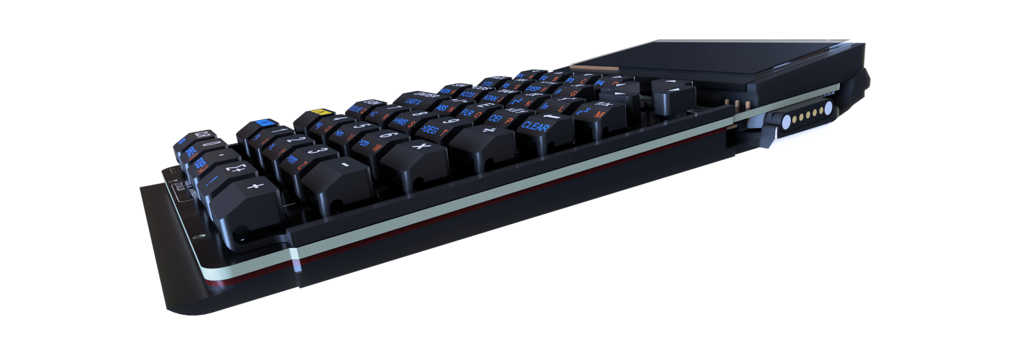
The most intricate part in the assembly is the key array. The array is modeled as a single piece for two primary reasons: per-part pricing from JLC3DP, and key stability while typing.
The previous version of this calculator had floating keys. These keys rattled easily and had a hard time centering on the switches underneath. The keys also tripled the production cost, as each key was $0.36, costing more than the case and back plate combined ($7). Floating keys also make it much more difficult to type on quickly.
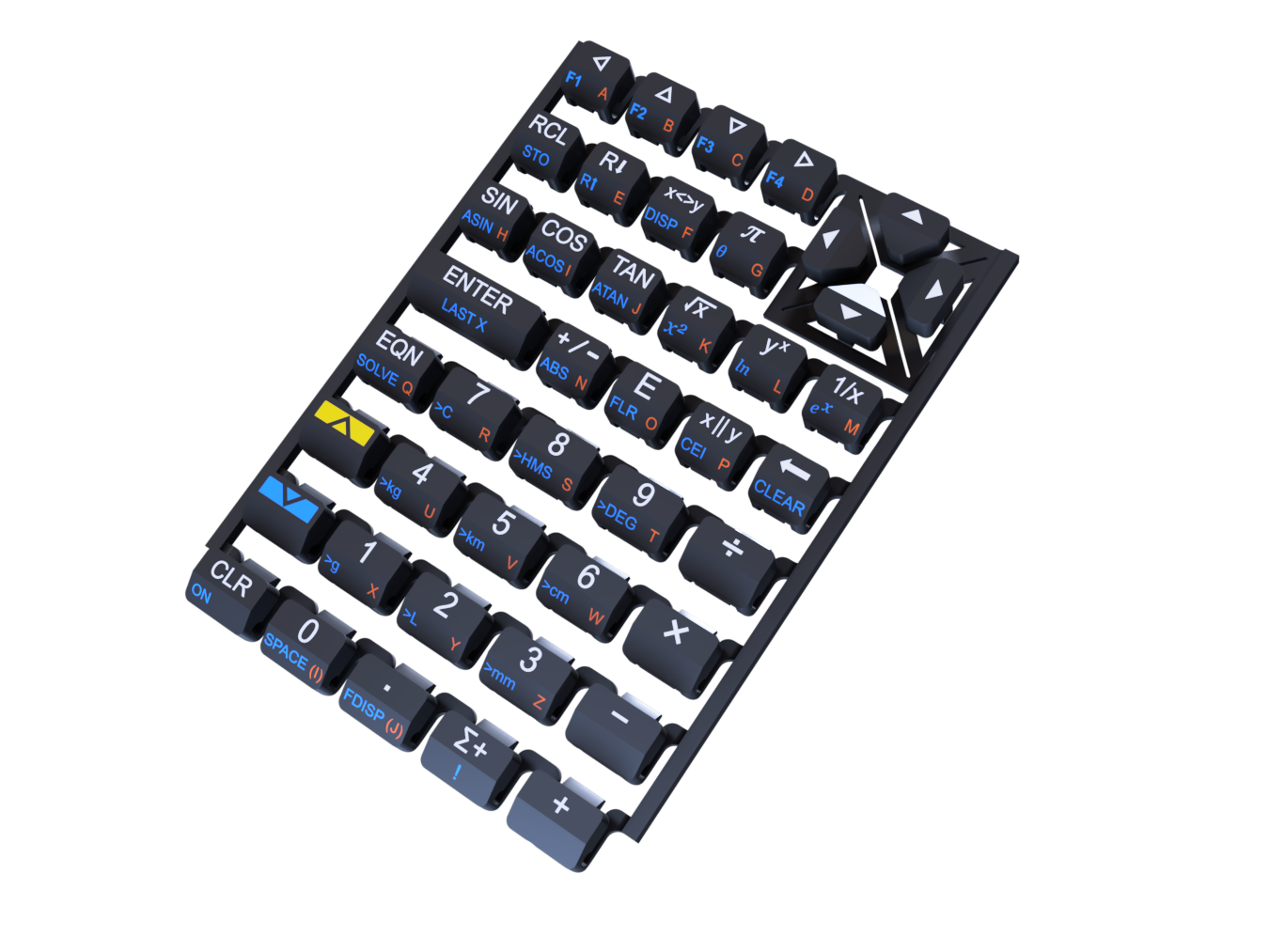
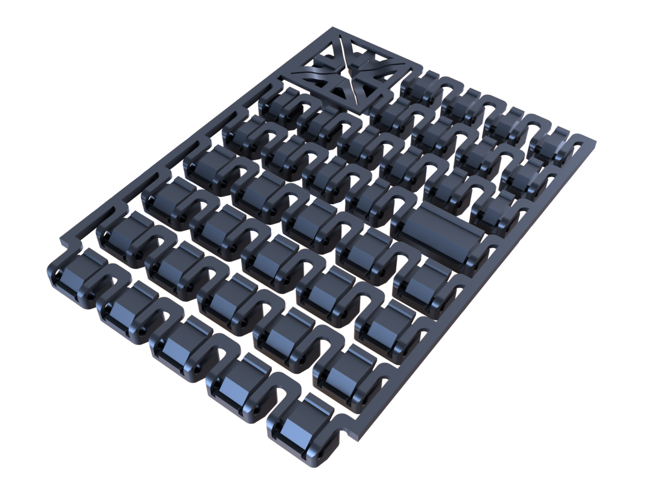
Labeling the keys presented a new set of challenges. SLA printing struggles to resolve tiny inset features as they can trap liquid resin, which will cure with the part. I ordered the key matrix with each key blank, and used Fusion360’s CAM tools to generate NC files to carve the keys with a 60 degree V cutter mounted to the head of my Prusa i3 MK3s.
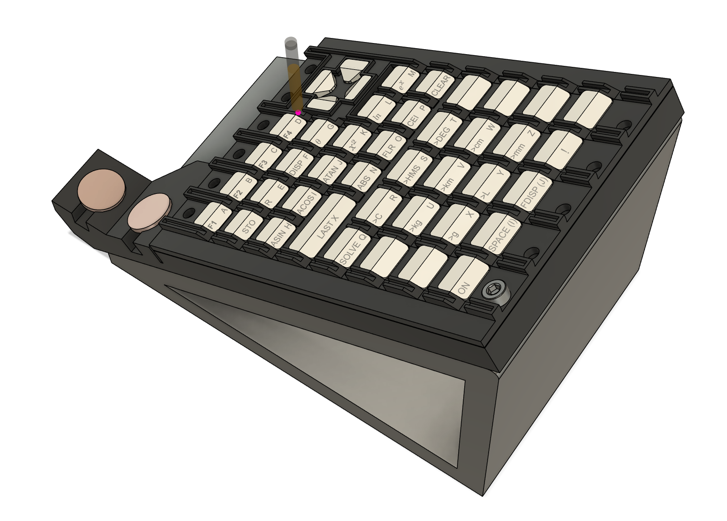
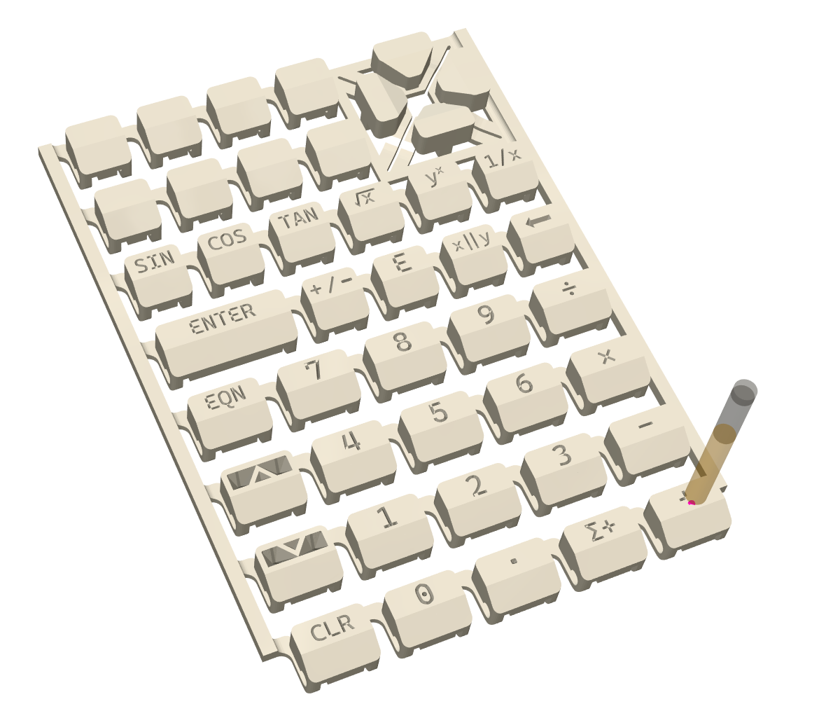
After carving the characters into the keys, the voids are filled with a lacquer stick to give contrast. An alternative method would be to use a silk screen stencil, but with the chamfered keys, this would have been difficult. An advantage to lacquer filled keys is that they will wear significantly more slowly, as the key face has to erode before the lacquer can be rubbed away.